Expected May 2027 · B.S. Electrical Engineering + B.S. Computer Engineering
Digital design from architecture to hardware bring-up.
I build RTL-heavy systems and take them through simulation, verification, synthesis, timing closure, FPGA integration, and lab validation. My recent work spans USB-PD protocol hardware, AES-GCM acceleration, a pipelined RV32I SoC, and a deep-capture FPGA logic analyzer.
SystemVerilogPrimary RTL language
20%FPGA logic reduction on AES-GCM
30%Latency reduction on AES-GCM
May 2027Graduation
SystemVerilog / Verilog
VHDL
AXI
SVA
CDC
Vivado
Quartus
C / C++
Python
Aug. 2026 – May 2027
Senior design project with Analog Devices: an FPGA-based logic analyzer built for configurable sampling, triggering, compression, and long-duration waveform capture. The architecture uses FPGA capture logic with DDR/DRAM-backed storage and processor-controlled data export.
Digital InputsConfigurable front-end interface
Capture RTLSampling, grouping, trigger logic
CompressionChange-based / RLE pipeline
DDR / DRAMDeep waveform buffering
ProcessorStorage and host export
SystemVerilog · Zybo Z7-10 · RISC-V
Designed a pipelined RV32I SoC with decode, ALU, register file, forwarding, load-use stalls, branch/jump flushing, dual-port BRAM, UART, LED MMIO, and FPGA bring-up.
Computer ArchitectureRTLFPGA
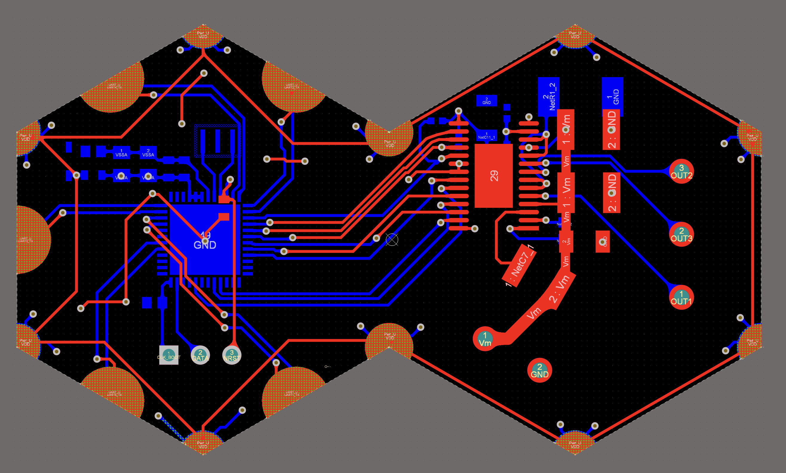
Designed a compact STM32 + DRV8313 sensored BLDC control module with separated power domains, high-current routing, decoupling, protection, and board-level verification.
PCB DesignEmbeddedPower
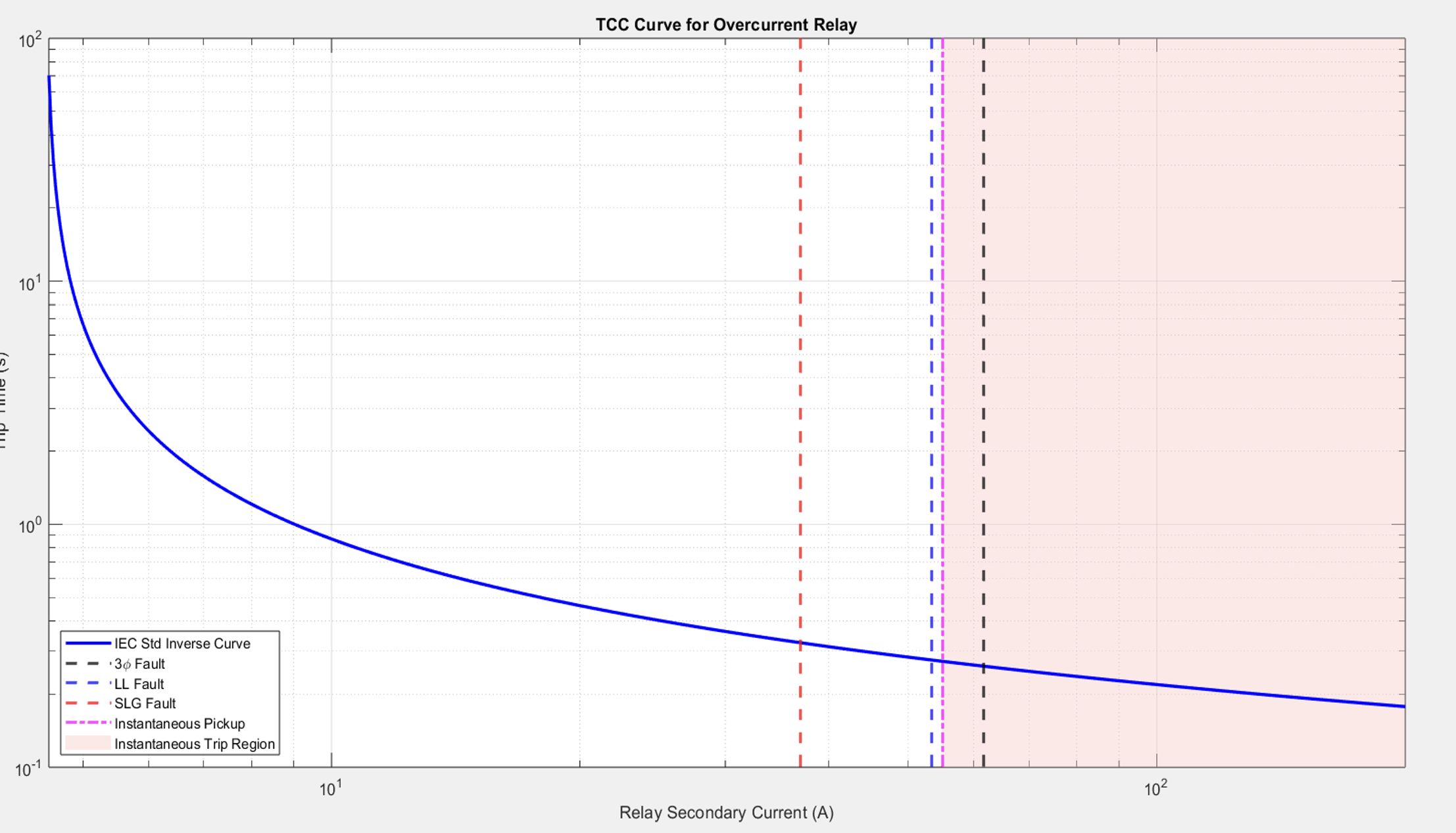
Built a MATLAB simulation of an IEC inverse-time overcurrent relay for a 13.8 kV feeder, generated TCC curves, and validated trip behavior across multiple fault types.
MATLABPower Systems
SystemVerilog · Vivado · Zybo Z7-10
Built small FPGA bring-up designs to validate the board clock, reset, GPIO, UART, and the Vivado implementation flow before integrating larger RTL systems.
VivadoSystemVerilog